
Apologies for such a long gap between posts. I meant to keep up with the sat rig project more closely but work and travel are doing a good job of getting in the way. Turns out, it’s not as easy as I thought to work on a large personal project while travelling all over the country for work.
In this episode of the DIY Sat Rig saga, we’re playing with real power. Well, 10 watts at least. The boards for the first revision of my amplifier design came in, and I just couldn’t wait to start finding out if my design was going to work (or if I was poised to be letting out a lot of magic smoke.)

I’ll add a disclaimer for this post – I’m no expert in the RF field, nor do I claim to be. This post will not be a step-by-step guide to amplifier design, nor will it go into great detail on a lot of the specifics. Partly because I’m not super qualified to lecture about design theory, but also to keep the reading relatively light and accessible to as many enterprising hams as possible (this article is long enough as it stands)
Small but Mighty
Before we start getting into the gritty testing details, let’s talk for a moment about the transistor I’m going to be using for these amplifiers.
I did a couple days’ worth of hunting around various distributors and manufacturers, looking for a chip that would be relatively easy to implement with minimal support circuitry. No fancy transformer matching or complex biasing, just something that could be, for the most part, “plug and play.” Much more common in high-power amplifiers like those made famous by W6PQL, LDMOS transistors are a great balance of high efficiency, small size, and simple operation. Of course, my amplifier isn’t going to be anywhere near the same caliber as Jim’s monstrous 2kW beasts, but we all have to start somewhere right?
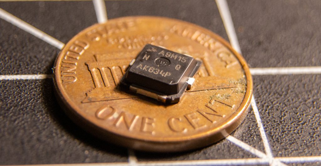
Eventually I stumbled upon NXP’s Airfast offerings. They’ve got LDMOS FETs that range from tiny 3W 7.5V chips all the way up to monster (relatively speaking) 70W jobs. Located somewhere in the middle is the AFT09MS015 – 15W out at 60% efficiency and running at 12.5V. It sounded like a perfect match! Digging through the datasheet, it had power, drive, and efficiency specs at VHF, UHF, and 800MHz and they all looked great. Input power was also specified to be approximately 200mW or so – almost exactly what the DRA818 modules put out in low-power mode! With everything coming together as well as it was, the decision had practically been made for me.
Just one problem – I’ve never designed a power amplifier before. It can’t be that hard, right?
Computers aren’t Cheating
Well, as it turns out it’s actually not all that hard – provided you have the right tools for the job. In decades past, if you wanted to design a new power amplifier module, you were in for a lot of experimentation. Load pull tests with the transistors you wanted to use, S-parameter sweeps under varying bias conditions, and a whole host of other calculations all had to be done before you could even think about working on a finalized design. The fact was that you didn’t have an easy way to get all the important RF performance data on a transistor without just trying (and failing) a bunch.

Luckily, nowadays things are much, much easier. Most of you might be familiar with SPICE – a simulation tool first developed in the early 90’s for analyzing circuits. It’s a fantastic tool with a lot of utility in the world of radio – but it does have its shortcomings. SPICE works mostly in the time domain, and it has rudimentary AC analysis capabilities, but when you’re talking amplifiers and non-linear devices in the RF world you’re gonna want something a little more built for the job. Enter microwave design packages – basically SPICE on steroids. There’s a bunch of different players in the game today – Keysight’s Advanced Design System, AWR’s Microwave Office, ANSYS’s Ansoft Designer, and the free packages Z0lver, Qucs, and Puff, just to name a few. Each one has its own following in the RF world, and each one has benefits and drawbacks depending on what you’re trying to do.
As it turns out, my new job has a site license for Keysight ADS and getting it installed on my computer was as simple as clicking “install” on the company intranet portal. That decided for me pretty quickly which design package I’d be using. It also helped that NXP offered a full ADS model package for the AFT09 which made things that much easier to get set up. I quickly learned, however, that just because you’ve got fancy design software and accurate models doesn’t mean you’re any more prepared when it comes down to the actual design part.
Find me a Match
Because things in life can’t be too easy, the input and output impedances of most RF transistors when biased are quite low; like 1-to-5-ohms low. Hooking that straight up to a 50Ω antenna or feedline is gonna give you lots of fun and interesting results1. So don’t do that. Instead, we need to build up a matching network for our transistor that can both bias it at the correct DC operating point and match the low input and output impedances to good ol’ 50Ω.

There’s a few main ways to go about doing this. The most popular method and the one found in most solid-state amplifier kits is using coaxial transformers on the input and output. These typically have a ratio2 of 9:1 or so which does a decent job of taking 50Ω down to 5(ish)Ω. The other big advantage of this type of matching is that it’s extremely wideband – you can typically get a decent amplifier match over the entire 3-30 MHz HF band. There are a couple drawbacks to transformer matching however – the biggest one being space constraints. Coaxial transformers, even when made with thin coax, are still relatively large – especially compared to small SMD capacitors and inductors. When board space is at a premium (as it is in this design) they’re not the most ideal option.
A much more space-conscious design, with the drawback of being far less wideband, is a traditional L-C matching circuit. These are super simple to implement, take up a tiny amount of board space, and can be made with off-the-shelf components to eliminate the need for hand-winding and hand-tuning. Since they’re resonant circuits, you’re not going to see a huge amount of bandwidth to the match, but for two single-band amplifiers like I’m designing it’s more than enough.
Fighting with Software
Alright, so that was a lot of background info. How about we actually get down to the gritty details and match ourselves up a transistor?
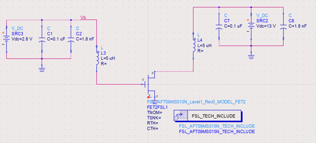
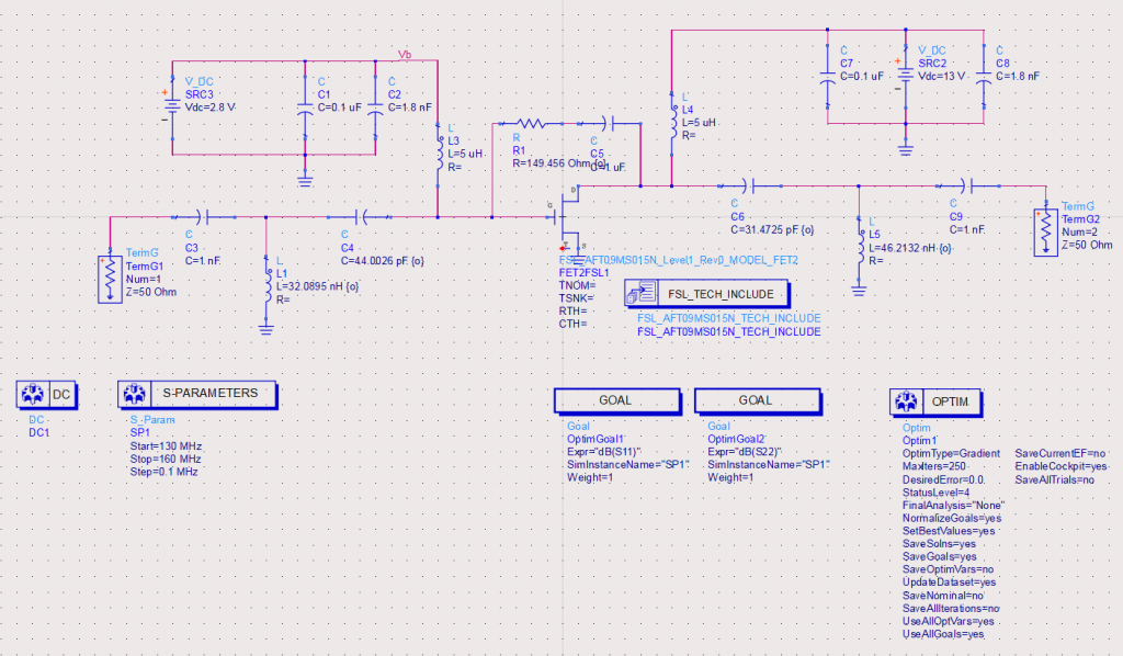
Like I mentioned earlier, NXP provides a full ADS model for the AFT09MS015. Once that was installed, I plopped it down in a new ADS project and started plugging away. First things first, we needed our DC bias circuitry. The FET needs a supply of 12.5V and a gate voltage that yields a quiescent current of 100mA3. I played around a little bit and found that a gate voltage of 2.8V got me reasonably close to the desired drain current I wanted. Other than that, to complete the DC section we just need some inductors to keep the RF from going where it’s not supposed to, and a couple capacitors to keep the DC supply relatively clean. That’s about it. Sadly the rest of the design wasn’t so easy.
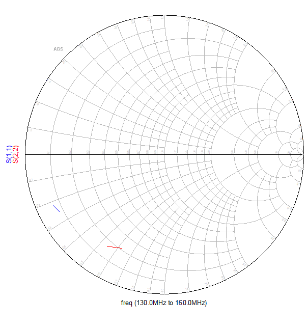
With the simple bits out of the way it was time to get down to some real work. What would happen if we just hooked the amplifier straight up to a radio in this state? Let’s go ahead and see what the input and output impedances look like right now. Adding in two S-parameter ports and setting up a simple sweep from 130-160 MHz shows us that our amplifier, in it’s current state, won’t work too terribly well.
So obviously we need to add in a matching network. Not only do we need to get those impedances nice and close to 50Ω; we also need to make sure that the DC biasing voltages don’t make their way into other places inside the RF chain, or really anywhere they shouldn’t be. There’s a couple different arrangements of capacitors and inductors you can use to do impedance matching, with the general idea being that you transform the low-impedance gate and drain of the MOSFET with series and parallel elements to get as close to 50Ω as you can. Now, the more academic among us might do some napkin calculations, choosing the right topology based on input and output impedances, and manually tuning for the final result. I took a slightly more brute-forced approach.
Optimization-ing Things
ADS has a fantastic built in feature known as the optimizer. It’s a beautiful tool that you can abuse to brute force your way towards a solution for many different circuits. UT Dallas has a fantastic intro lab on the basics of the optimizer that I used as a starting point for my simulation (the optimization-specific section starts on page 12). Essentially, you can specify weighted goals that can be almost any variable in the circuit, and components that can be optimized. You give these components ranges of values they can be, and hit the big optimize button. Depending on processing power and whether or not your goals are even physically possible, when the tool is done you’ll have a pretty darn good result.
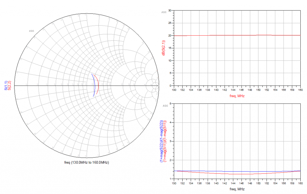
In my case, I specified two goals: return losses at S1 and S2 of at least 20dB (which works out to an SWR of around 1.2). Since the amplifier is already held constant at a certain bias point, making sure the input and output are matched is the only other big thing that needs to be done (besides filtering – we’ll get to that).
Remember earlier when I was talking about matching topologies? Well, I was struggling to get a good match with any of the ones I mentioned before. Pi, Tee, and any variations thereof weren’t giving me the match I wanted (or really any good match at all) and I spent two evenings struggling to get something usable. There’s probably an analytical reason for this, or I might’ve just not been approaching it the right way. Or maybe I was just using ADS wrong, who knows.
Doing some heavy research one evening, I stumbled upon an article written by Paul Wade, W1GHZ, on simple amplifier matching. Aptly titled Simple Broadband Solid-State Power Amplifiers, it discusses a novel way to match an amplifier using nothing more than a resistor and capacitor. While it didn’t give me a perfect match right off the bat, using the resistor feedback along with two L networks on the input and output of the MOSFET immediately showed better results in the optimization. After letting it crunch for a little while, I had a great looking match with flat SWR across the whole 2m band, and great theoretical gain to boot!
After following basically the same approach above for the 70cm amplifier, I had a potentially viable design for both bands and was ready to start the much more fun part – physical testing!
Welcome to the Real-World
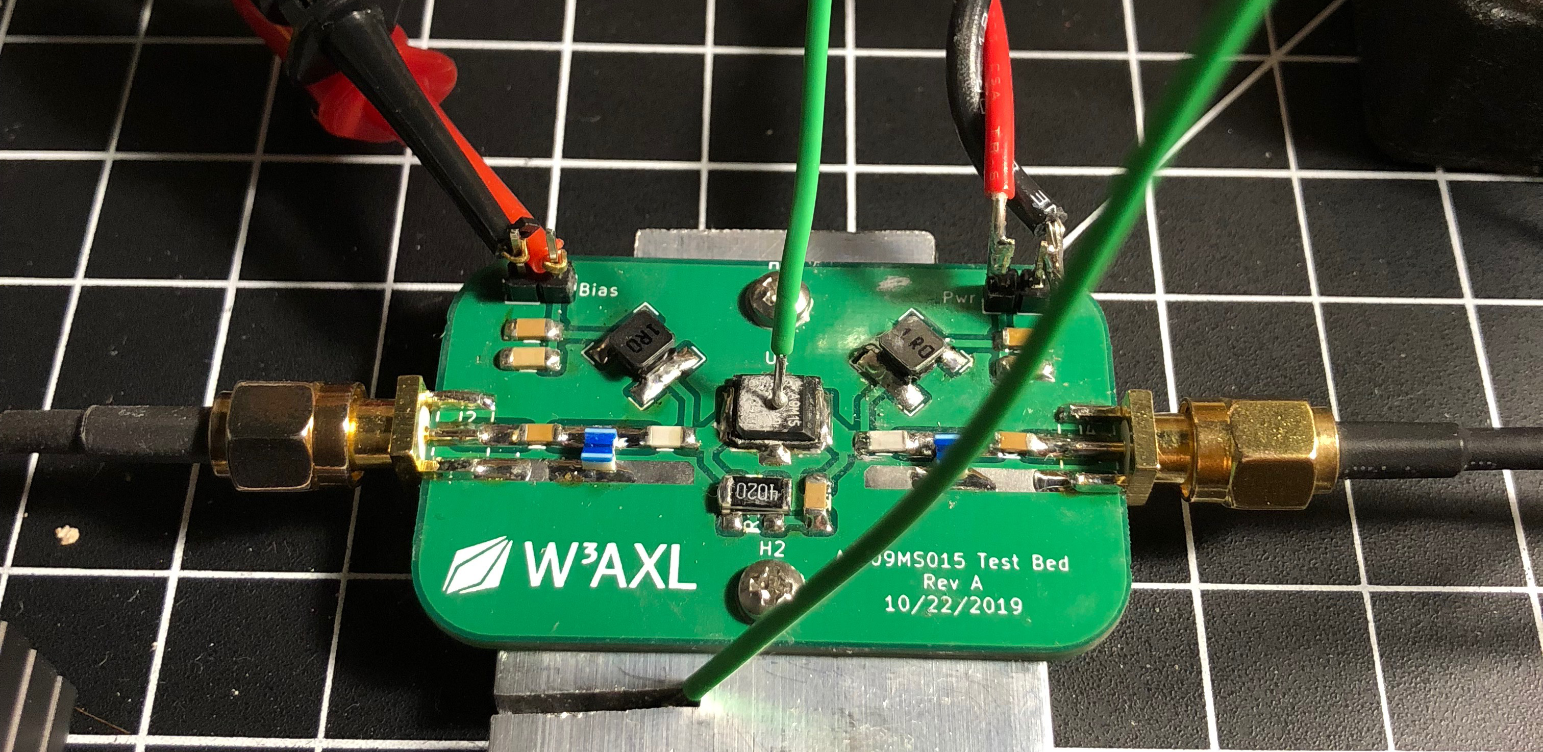
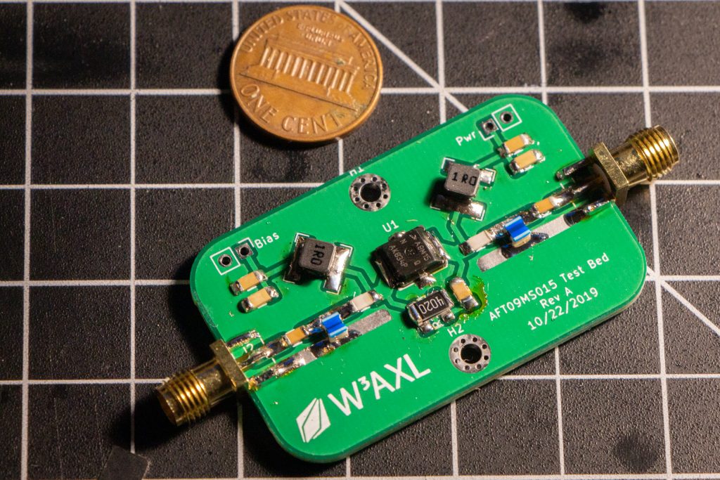
With all the un-fun simulations and calculations done, we’ve got a workable design to test out. I spun up a quick PCB via my new favorite fab house JLCPCB4 and ordered the parts from Digikey. The board is super simple – just some CPWG5 tracks on the amplifier input and output, exposed to allow for placement of capacitors and inductors wherever necessary. The DC side of things has inputs for power and bias voltage, filtered with a few capacitors and connected via big inductors to the RF lines. Input and output RF lines terminate in SMA connectors. Like I said, simple. Just enough on the board to do some basic testing. In a week everything was at my door and we were ready to start some real testing.
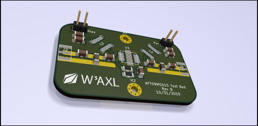
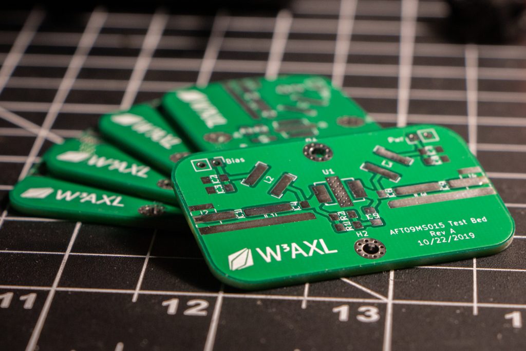
Soldering the thing up was relatively straightforward. The PLD-1.5W package is a little awkward to get attached to the ground plane, and I’ll probably make the pads a little bigger on the footprint to make it easier to get soldered. You can also see how I made the bias-tee inductor footprints just a little bit too big.
So now we’re down to the meat of it all: how does the amplifier actually perform?
Testing, Testing, 1, 2, 3rd Harmonic
The test setup for this amplifier was super simple: 12V supply for power, 2.8V adjustable supply for the bias, input from the DRA transceiver module6, and output into my HP 8935 as a spectrum analyzer. I set up a fairly dirty thermal solution with some aluminum bar stock, and threw thermocouples on the IC case and the “heatsink” to see what my temperatures looked like.
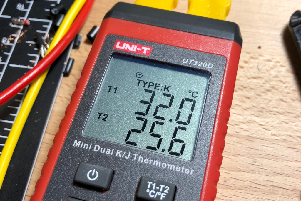
With my safety squints (and a conservative current limit on the power supply) engaged, I powered up the amplifier and started bringing up the gate bias voltage. Nothing let the smoke out, and I didn’t see any weird oscillations on the spectrum analyzer. I watched the drain current rise to around 90mA (close enough to the theoretical 100mA the datasheet called for) and the case temperature settled at a very modest 32C. So far so good!
Of course, the amplifier wasn’t actually doing any amplifying yet. The real test would be once I keyed up the DRA module. With my fingers crossed and a fire extinguisher on standby, I hit PTT.
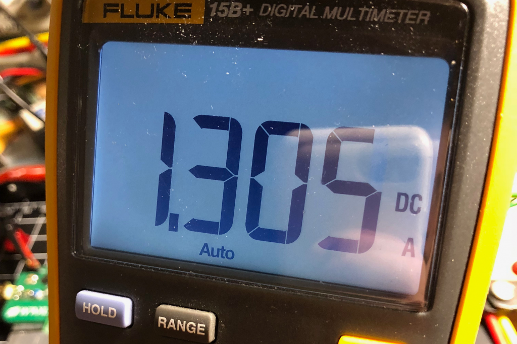
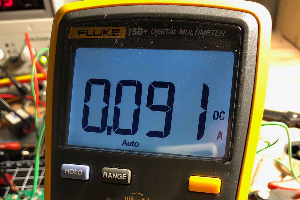
Current immediately jumped up to around 1.3A, and I saw the temperatures climbing. Something was happening, but was it good? Well, let’s glance over at the specan screen to see what’s going on (with a 100MHz to 900MHz span):
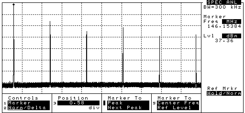
I mean, that’s at least an amplified signal. The fundamental’s power was hovering just around 37.5dBm which is equivalent to approximately 5.6W of power out. The second harmonic, however, was only about 13dB down at 24.5dBm (282mW), and the rest were sitting between 10-20dBm. Of course, this is the output with absolutely no filtering of any kind so I wasn’t expecting super clean results. Still, there’s a decent amount of power in those harmonics
Continuing the investigation, I hooked up the spec an directly to the output of the DRA module, just to see what its spectrum looks like. These cheap Chinese modules are known to not have the best harmonic response, so I was curious how much of that harmonic content was coming from the radio itself.
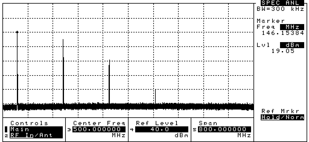
So obviously the DRA isn’t the cleanest radio in the world either. However, I’ve got some higher-order harmonics coming from somewhere7 that need to be dealt with. As I hinted to above, the final RF design does include a frontend lowpass filter which should at least make the transmitter output legal. Still, I’d like to try and figure out where those products are coming from.
Efficiency and Other Things
Switching gears, even with the (in my opinion) horrid harmonics the amp was putting out, I wanted to see what the total overall efficiency looked like. Using the RF analyzer of the 8935, I checked what my DRA module was putting in, as well as what the amplifier was putting out.
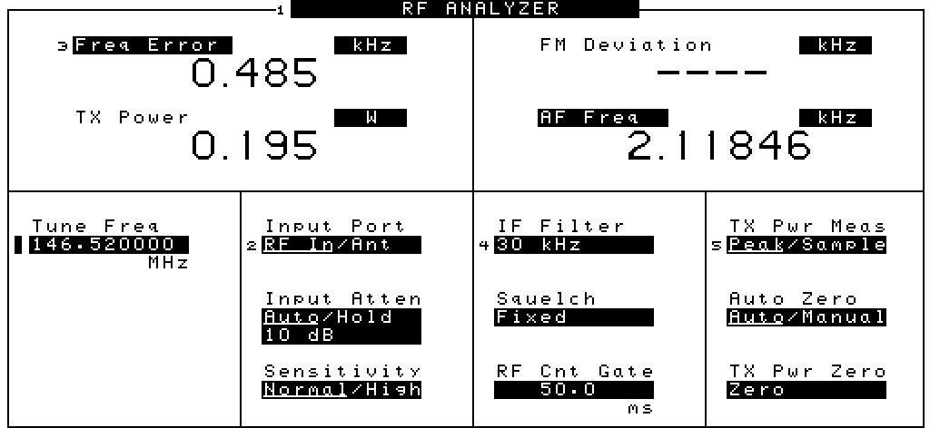
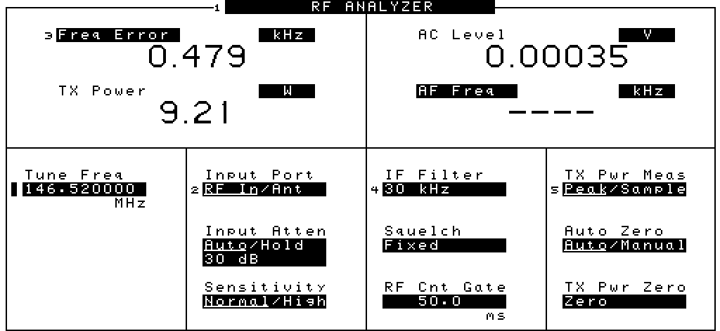
So when we take into consideration the overall Pout vs Pin, the amplifier actually doesn’t look too bad. 0.2W to 9.2W is a gain of 16.6dB, pretty much exactly what the AFT09’s datasheet said to expect at VHF. Efficiency wasn’t too bad either; 1.3A at 12V is 15.6W, and with the input power our total power consumption is 15.8W. With 9.2W out, that’s an efficiency of 58% compared to the datasheet’s 60%. All in all, considering that this is an amplifier circuit that was designed and built in less than a week those results aren’t too bad at all.
Where to next?
So, I think at this point it’s safe to say that my amplifier design is definitely viable. That’s great news for the sat rig project, because it’s one of the major hurdles in the design of the RF board and I’m happy to have at least a working “revision A” prototype. Obviously filtering is going to be of particular concern in future designs, and I’ll probably do one more test bed PCB with input and output filtering just to make sure that it’s not something else causing my problems like clipping or strange nonlinearities.
Stay tuned for the next post about the satellite rig! Until then, keep tinkering and 73!
- I tried to find pictures of amplifiers burning up from high SWR faults but surprisingly couldn’t
- impedance ratio!
- from the NXP datasheet for bias conditions
- I’m not paid by them or anything but go check out their pricing on boards – it’s pretty impressive
- Coplanar Waveguide with Ground
- because my signal generator output power didn’t go high enough
- if you have any ideas as to where they’re coming from, I’m all ears. I suspect it’s either nonlinear weirdness or some mixing going on somewhere
Hi, thank you for publishing your experiments. I’m learning a great deal about impedance matching on RF amplifiers from this. Did you check out SimSmith software? It’s free and helped me to do some simple practical impedance matching. There are also a lot of explaination about this software on Youtube. Good luck constructing your TRX. I hope you succeed. I guess you’re going to use 2 power decks, 1 for each band as the impedance network restricts you from using 1 deck for both bands? Or are you going to do a clever trick with some pin diodes? I’m curious how much the signal will cleanup if you only use a lpf at the input.
Are you going to use a 5 pole chebyshev network again like you did on the panadapter tap?